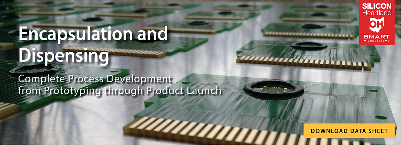
Encapsulation of microsystems is a sophisticated process requiring understanding of the encapsulant materials and their interactions with die surfaces, package substrates and their related processes, as well as the physical environment in which the packaged device will be exposed. The encapsulation capabilities and expertise at SMART Microsystems support the process development, testing, and manufacturing of sub-assemblies designed by our customers allowing them to quickly realize a microelectronic package assembly solution for their products. For additional information you can call or send us an email to discuss your encapsulation needs.

LID SEAL SPECIFICATIONS
•   Solder, epoxy, tape
•   Hermetic and non-hermetic
•   TO headers, DIP packages, open cavity plastic packages, ceramic packages

PARYLENE COATING SPECIFICATIONS
•   Chamber Size 12 inch dia. X 12 inch high (8.5”/31.5cm dia. X 11.19”/28.4cm H, useable size)
•   Dimer Capacity 125 grams
•   Cold Trap using Mechanical Chiller
•   Deposits Parylene type C at 0.0002” per hour
•   Deposits Parylene type N at 0.00003” per hour

ADHESIVE DISPENSE SPECIFICATIONS
•   Dam and fill
•   Glob top
•   Potting
•   Epoxies, heat cures, UV cures, thixotropic adhesives
•   Time/pressure dispense, auger dispense, and jetted dispense
•   Weight controlled dispensing
•   X-Y repeatability: ±25µm
•   Z-axis repeatability: ±25µm
•   X -Y Travel: 525 x 525 mm (20.7 x 20.7 in.)
•   Z Travel: 75 mm (2.95 in.) maximum