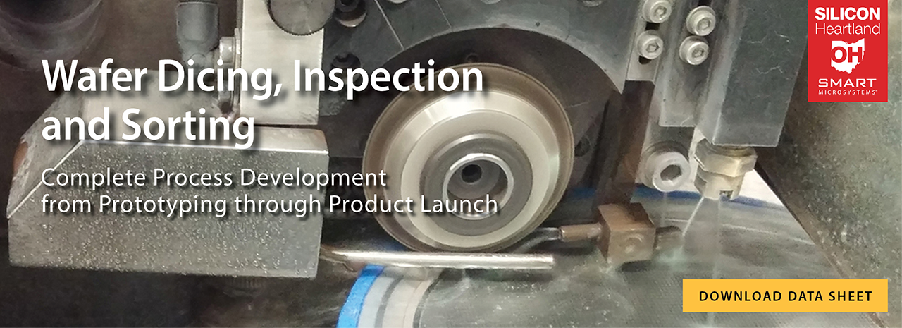
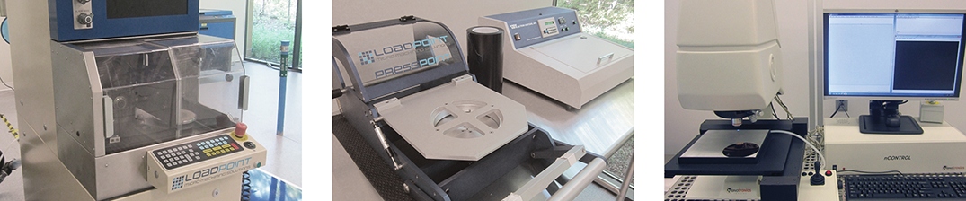
Dicing is the process in which semiconductor wafers such as MEMS and IC’s are singulated into individual die before package assembly. This is an automated process to ensure precision and accuracy. Depending on the substrate material and thickness, we use different dicing blade thicknesses and materials to saw wafers. Our dicing services include wafer inspection and die sorting if required. Diced wafers can be shipped on the tape hoop, or sorted into waffle pack or Gel-pak. For more information you can call or send us an email to discuss your wafer dicing needs.

WAFER INSPECTION SPECIFICATIONS
•   Stage accommodates up to 200 mm wafers
•   Typical image size 2752 x 2200 pixels with 4.54 μm resolution per pixel with repeatability ± 2 μm
•   Brightfield/Darkfield Optics at 2.5x and 5x with high spatial resolution camera imaging 19 fps
•   Automatic reporting generated includes defect density maps and defect count histograms
•   Software includes Die Yield Analyzer for patterned wafer recognition
•   Programmable automatic quantification and qualification of features of interest
•   Programmable automatic and manual image capture parameters of focus, lighting, magnification, and movement

DIE SORT SPECIFICATIONS
•   Die size: ≥0.17mm square and up
•   Die thickness: ≥0.020mm
•   Max wafer size: 300mm

WAFER DICING SPECIFICATIONS
•   Max wafer size: 6” diameter (round or square) and up to 10mm thick
•   Utilizes tape rings or grip rings to hold materials
•   Performs cutting, dicing and scribing operations
•   Spindle speeds: 3,000 to 60,000 rev/min
•   Resolution of the axes:
•   X Axis – 0.1 mm
•   Y Axis – 100 nanometres
•   Z Axis – 100 nanometres
•   Theta axis: 6 million lines; 0.0004 ° resolution
•   Dicing speed: 0.1-500mm/sec
•   Videoscope alignment uses either pattern recognition or vision system two-point alignment
•   Blade capacities: 50mm to 76.2mm
•   Range of materials includes Alumina, BGA and CBGA moldings, Ceramic, Glass, Lead, Zirconate Titanate, Fibre Board and Silicon